Multi-Node GPU Collective Communication Architecture: NVLink 5 Fabric Switch Topologies, NCCL Ring vs. Tree AllReduce, and GPUDirect RDMA BAR1 Memory Mapping
An institutional systems architecture analysis of distributed GPU collective communication primitives, examining NVLink 5 1.8 TB/s non-blocking switch fabrics, NCCL Ring versus Double-Binary Tree AllReduce latency scaling, PCIe BAR1 GPUDirect RDMA peer-to-peer DMA, and in-network SHARP aggregation.
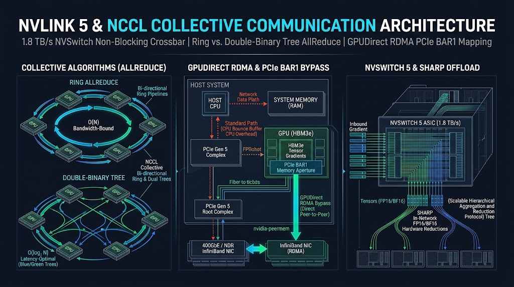
In large-scale distributed tensor computation and frontier foundation model training across thousands of accelerators, cluster utilization—measured as Model Flops Utilization (MFU)—is governed not by peak streaming multiprocessor (SM) compute throughput, but by the tail latency and bisection bandwidth of synchronous collective communication primitives. During each backward pass under Fully Sharded Data Parallelism (FSDP) and 3D Tensor/Pipeline Parallelism, gigabytes of bfloat16/fp8 parameter gradients must be synchronized across intra-node high-bandwidth domains and inter-node network fabrics via AllReduce, AllGather, and ReduceScatter operations. Eliminating host CPU memory-copy bottlenecks and network serialization stalls requires coordinating NVLink 5 / NVSwitch non-blocking crossbar topologies, NVIDIA Collective Communications Library (NCCL) Ring versus Double-Binary Tree algorithms, GPUDirect RDMA PCIe Base Address Register (BAR1) peer-to-peer mapping, and Scalable Hierarchical Aggregation and Reduction Protocol (SHARP) in-network switch arithmetic.
1. Intra-Node Scale-Up Fabrics: NVLink 5 SerDes & Non-Blocking NVSwitch Crossbars
Traditional PCIe Gen 5.0 ($\times 16$ bidirectional bandwidth of $128\text{ GB/s}$) and PCIe Gen 6.0 ($256\text{ GB/s}$) host interconnects represent an immediate serialization bottleneck when synchronizing High-Bandwidth Memory (HBM3e) stacks operating at $8.0\text{ TB/s}$ per accelerator. Furthermore, traversing the host CPU's PCIe Root Complex introduces non-uniform memory access (NUMA) coherency overhead and cache-line snoop traffic that degrades multi-GPU collective scaling.
To establish a flat, cache-coherent scale-up memory domain across $8$ to $72$ accelerators, modern GPU compute nodes deploy dedicated NVLink 5 high-speed differential SerDes lanes coupled with external NVSwitch ASICs. Each NVLink 5 bidirectional sub-link operates using $200\text{ Gbps}$ 4-Level Pulse Amplitude Modulation (PAM4) signaling across two differential pairs per direction, delivering $100\text{ GB/s}$ per link—or $1.8\text{ TB/s}$ of aggregate bidirectional bandwidth across $18$ links per GPU. Rather than wiring GPUs in a direct point-to-point torus or hypercube (which requires multi-hop store-and-forward routing), NVSwitch chips form a fully provisioned, non-blocking Clos crossbar fabric where any GPU can issue direct load/store memory transactions or asynchronous DMA copy descriptors to any peer GPU's HBM3e physical address space at full wire speed.
$$T_{\text{Ring}}(N, M) = 2(N - 1)\,\alpha_{\text{hop}} + \frac{2(N - 1)}{N} \cdot \frac{M}{B_{\text{bottleneck}}} + \frac{(N - 1)}{N} \cdot M \cdot \gamma_{\text{ALU}}$$ Where $\alpha_{\text{hop}}$ is per-step link startup latency, $B_{\text{bottleneck}}$ is the slowest unidirectional link bandwidth in the logical ring, and $\gamma_{\text{ALU}}$ is per-byte element-wise reduction cost. As $N \to \infty$, bandwidth volume converges to the optimal lower bound $2M / B_{\text{bottleneck}}$, but latency scales linearly as $\mathcal{O}(N)$.
$$T_{\text{Tree}}(N, M) = 2\left(\log_2 N\right)\alpha_{\text{hop}} + 2\left(\frac{M}{B_{\text{link}}}\right), \qquad T_{\text{SHARP}}(N, M) = 2\left(\log_k N\right)\alpha_{\text{switch}} + \frac{M}{B_{\text{NIC}}}$$ Double-binary trees reduce latency complexity from $\mathcal{O}(N)$ to $\mathcal{O}(\log_2 N)$ at large cluster scales ($N \ge 256$), while switch-based SHARP cuts aggregate network payload transfers in half ($2M \to M$).
2. Algorithmic Collectives: NCCL Ring vs. Double-Binary Tree AllReduce Mechanics
In distributed data-parallel synchronization, the NVIDIA Collective Communications Library (NCCL) dynamically constructs topology-aware communication graphs by probing the system's PCIe, NVLink, NUMA, and RDMA NIC hierarchy via XML topology discovery. For an AllReduce operation over a gradient tensor of size $M$ bytes across $N$ ranks, NCCL selects between three core transport topologies depending on payload size and cluster diameter:
- Bandwidth-Optimal Ring AllReduce ($N-1$ Scatter-Reduce + $N-1$ AllGather Steps): The tensor $M$ is partitioned into $N$ contiguous chunks of size $M/N$. In Phase 1 (
ReduceScatter), each GPU $i$ transmits chunk $(i - k) \pmod N$ to rank $(i + 1) \pmod N$ while receiving chunk $(i - k - 1) \pmod N$ from rank $(i - 1) \pmod N$ and executing an in-place vector addition across $N - 1$ steps. In Phase 2 (AllGather), the fully reduced chunks circulate around the ring in another $N - 1$ steps. While Ring AllReduce achieves $100\%$ link bandwidth utilization for massive messages ($M > 64\text{ MB}$), its $2(N - 1)$ sequential hop latency degrades severely when $N$ scales past $128$ nodes. - Complimentary Double-Binary Tree AllReduce: To eliminate the $\mathcal{O}(N)$ latency penalty without sacrificing full-duplex bandwidth, NCCL constructs two interleaved binary trees across the same $N$ ranks: in Tree A, even-numbered ranks act as interior parent nodes ($50\%$ duplex load) and odd-numbered ranks act as leaf nodes; in Tree B, the roles are inverted so odd-numbered ranks become interior parent nodes and even-numbered ranks become leaves. Splitting the tensor $M$ into two halves ($M/2$ on Tree A, $M/2$ on Tree B) achieves simultaneous full bidirectional bandwidth utilization with logarithmic $\mathcal{O}(\log_2 N)$ hop latency.
- NVLS (NVLink SHARP) & CollNet (In-Network Switch Reductions): Rather than executing floating-point additions inside GPU SMs (which steals warp scheduler slots and L2 cache bandwidth from matrix multiplication kernels), NVSwitch v3/v4 and InfiniBand/RoCE SHARP switches embed dedicated Floating-Point Reduction ALUs directly inside the switch silicon. Each GPU transmits its gradient buffer once ($1\times M$) into the switch multicast group; the switch ASIC accumulates the vectors in flight and broadcasts the final reduced result back to all participating GPUs, cutting inter-node network traffic by $50\%$.
3. Comparative Architecture of Collective Communication Topologies
Systems architects evaluate multi-node GPU synchronization protocols across five latency, bandwidth-multiplier, and hardware-offload dimensions:
| Collective Algorithm | Hop Latency Scaling | Per-Rank Data Volume | SM Compute Overhead | Optimal Cluster Regime |
|---|---|---|---|---|
| 1D Ring AllReduce | $\mathcal{O}(2N - 2)$ sequential steps | $2 \left(\frac{N-1}{N}\right) M \approx 2M$ | $4\text{ to }16$ GPU SMs (LL/Simple protocols) | Small-to-medium clusters ($N \le 64$), large tensors ($M \ge 128\text{ MB}$) |
| Double-Binary Tree | $\mathcal{O}(2 \log_2 N)$ tree depth | $2M$ (split $M/2$ across 2 trees) | $4\text{ to }16$ GPU SMs | Large-scale multi-rack clusters ($N \ge 128\text{ to }16,384$ GPUs) |
| 2D Hierarchical (NVLink + Ring) | $\mathcal{O}(N_{\text{nodes}} + G_{\text{local}})$ | $2M / G_{\text{local}}$ across inter-node NIC | Moderate SM usage | Asymmetric intra-node NVLink vs. inter-node RoCEv2 bandwidth |
| NVLS / InfiniBand SHARP | $\mathcal{O}(2 \log_k N)$ switch radix | $1.0 \times M$ ($50\%$ traffic reduction) | $< 2$ GPU SMs (Offloaded to Switch ALU) | NVSwitch v3/v4 domains & SHARP-enabled InfiniBand fabrics |
4. GPUDirect RDMA: PCIe BAR1 Aperture Mapping & `nvidia-peermem` Kernel Mechanics
When a collective operation crosses physical server boundaries over 400GbE RoCEv2 or NDR InfiniBand, standard networking paths copy GPU HBM buffers into pinned host system DRAM (`cudaMallocHost`) across the PCIe bus before the Network Interface Card (NIC) DMA engine can transmit the packet—doubling PCIe traversal latency and saturating the CPU's integrated memory controller.
GPUDirect RDMA eliminates host DRAM bounce buffers entirely by enabling a third-party PCIe device (such as a ConnectX-7/8 RDMA NIC) to execute peer-to-peer DMA reads and writes directly against GPU High-Bandwidth Memory over a dedicated PCIe switch hierarchy:
- PCIe Base Address Register (BAR1) Aperture Exposure: The GPU exposes a programmable sliding window (or full 64-bit resizable BAR1 aperture on modern server platforms) of its internal HBM3e physical memory into the host system's 64-bit physical PCIe MMIO address space.
- Kernel Peer-Memory Registration (
nvidia-peermem/dma-buf): When NCCL registers a GPU tensor buffer via the InfiniBand Verbs API (ibv_reg_mr()oribv_reg_dmabuf_mr()), the Linux RDMA core subsystem invokes thenvidia-peermemkernel module (or standard Linux kerneldma-bufsubsystem). This pins the GPU's physical HBM pages and populates the NIC's on-board Memory Translation Table (MTT) with the exact PCIe BAR1 physical bus addresses. - PCIe Root-Complex Bypass via Dedicated Switch Complexes: Because traversing a CPU's internal PCIe Root Complex for peer-to-peer DMA transactions often degrades throughput into fragmented 64-byte completion packets, production AI servers co-locate each GPU and its dedicated 400GbE/NDR NIC beneath a shared PCIe Gen 5/6 Switch ASIC with PCIe Access Control Services (ACS) P2P redirection disabled—guaranteeing full-rate zero-copy DMA transfers directly between the NIC wire and GPU HBM3e.
Primary High-Performance Computing & Hardware Interconnect References
- 1. NVIDIA Developer Documentation: GPUDirect RDMA Architecture — PCIe BAR1 Peer-to-Peer DMA Mapping & Linux Kernel `nvidia-peermem` Interface Specification.
- 2. NVIDIA Collective Communications Library (NCCL): NCCL Topology Discovery, Ring vs. Tree AllReduce Protocols (LL, LL128, Simple), and NVLS Collectives.
- 3. IEEE Micro / High-Performance Interconnects: Scalable Hierarchical Aggregation and Reduction Protocol (SHARP) — In-Network Switch Arithmetic for Exascale Collective Offload.
Related Systems & Network Architecture Research
TrendSpike Editorial Team
Staff Research & Technical AnalysisIndependent research covering distributed cloud systems, modern enterprise software engineering, and macro-financial policy. Our technical and financial analyses reference primary documentation, official regulatory filings, and benchmark architectures.